Measurement of the Melting Point of Hexagonal Boron Nitride under Pressures below 5 GPa
-
摘要: 设计并组装了一套瞬间放电装置,实现了样品在DS 6×14 MN国产铰链式六面顶大腔体压机下的高压瞬间放电加热。结合大腔体静高压加载技术以及瞬间放电加热技术,利用熔体凝固过程中晶体经历形核和生长2个阶段的特征,判断晶体的熔化情况。对h-BN粉晶进行了高压环境下的瞬间放电加热处理,以研究高压下h-BN的熔化行为。采用扫描电子显微镜对高压条件下经历瞬间放电加热处理的样品进行微观形貌分析,判断h-BN晶体的熔化情况,确定了在3.4和4.3 GPa压力下h-BN的熔点分别为(
4251 ±150) K和(4531 ±200) K。这些发现有利于h-BN的应用探索以及现有氮化硼高温高压相图的修正。Abstract: In this study, a flash-heating device was designed and assembled to achieve instantaneous discharge heating of samples under high pressure in the DS 6×14 MN domestic hinged six-anvil large chamber press. By combining large chamber static high pressure and instantaneous discharge heating technologies, the melting state of crystals has been determined by the nucleation and growth characteristics during solidification. The melting behavior of h-BN powder crystal under high pressure was studied by instantaneous discharge heating treatment. Using scanning electron microscopy (SEM), the microstructures of samples obtained by high-pressure instantaneous discharge heating treatment was analyzed in order to assess the melting state of h-BN crystals. It was determined that the melting points of h-BN under 3.4 and 4.3 GPa are (4251 ±150) K and (4531 ±200) K, respectively. These results are beneficial for exploring the applications of h-BN and revising the existed temperature-pressure phase diagram of boron nitride. -
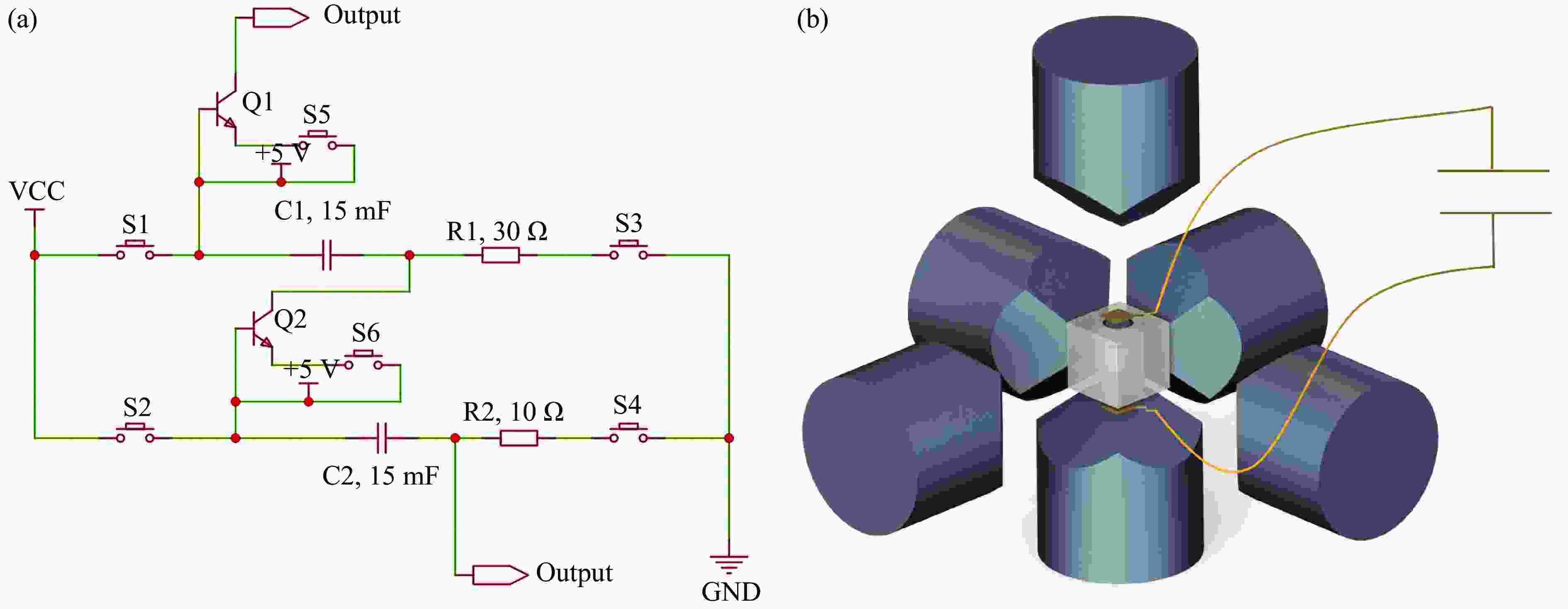
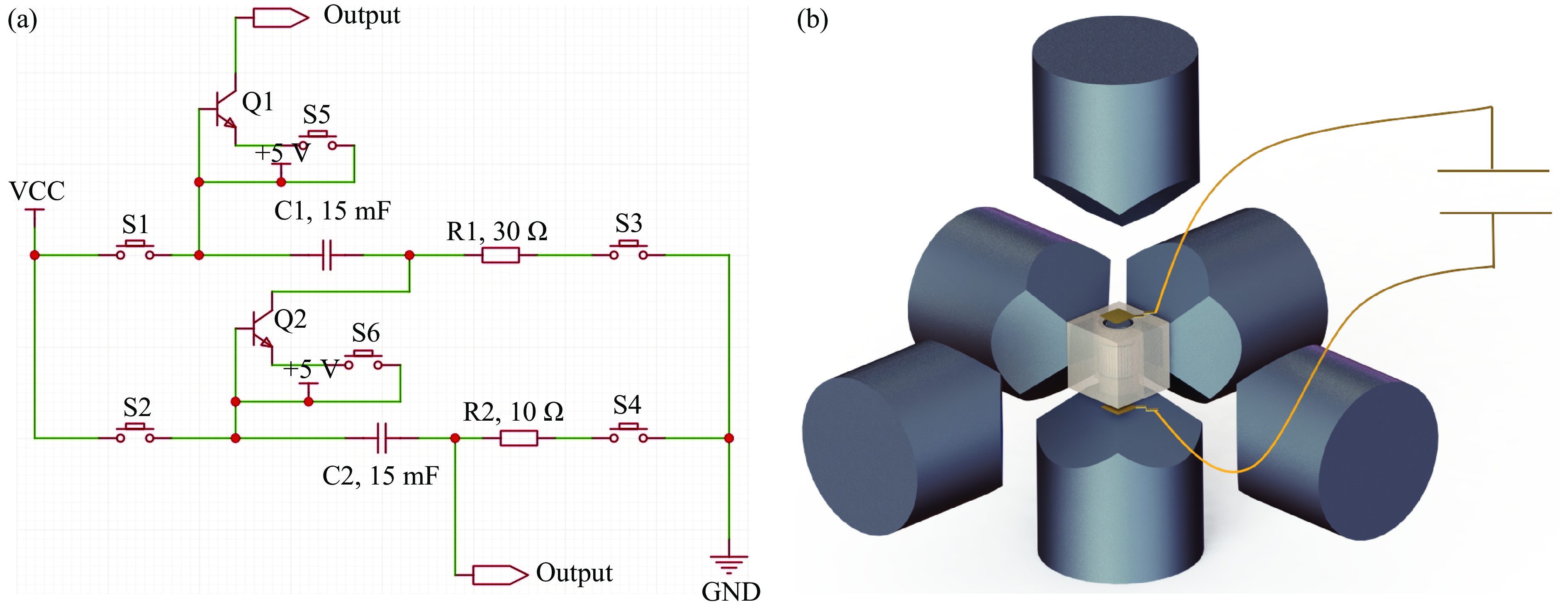
图 1 瞬间放电装置内部电路 (a) 以及组装连接 (b) 示意图(使用10 AWG粗导线连接,并联的电容分为上级电容和下级电容,最大输出电压为1 kV,不能同时充放电)
Figure 1. Schematic diagrams of the internal circuit (a) and connection assembly (b) of the flash-heating device (The capacitors are arranged in parallel by using 10 AWG thick wires and divided into upper-level and lower-level. The maximum output voltage is 1 kV. Simultaneous charging and discharging are not permissible.)
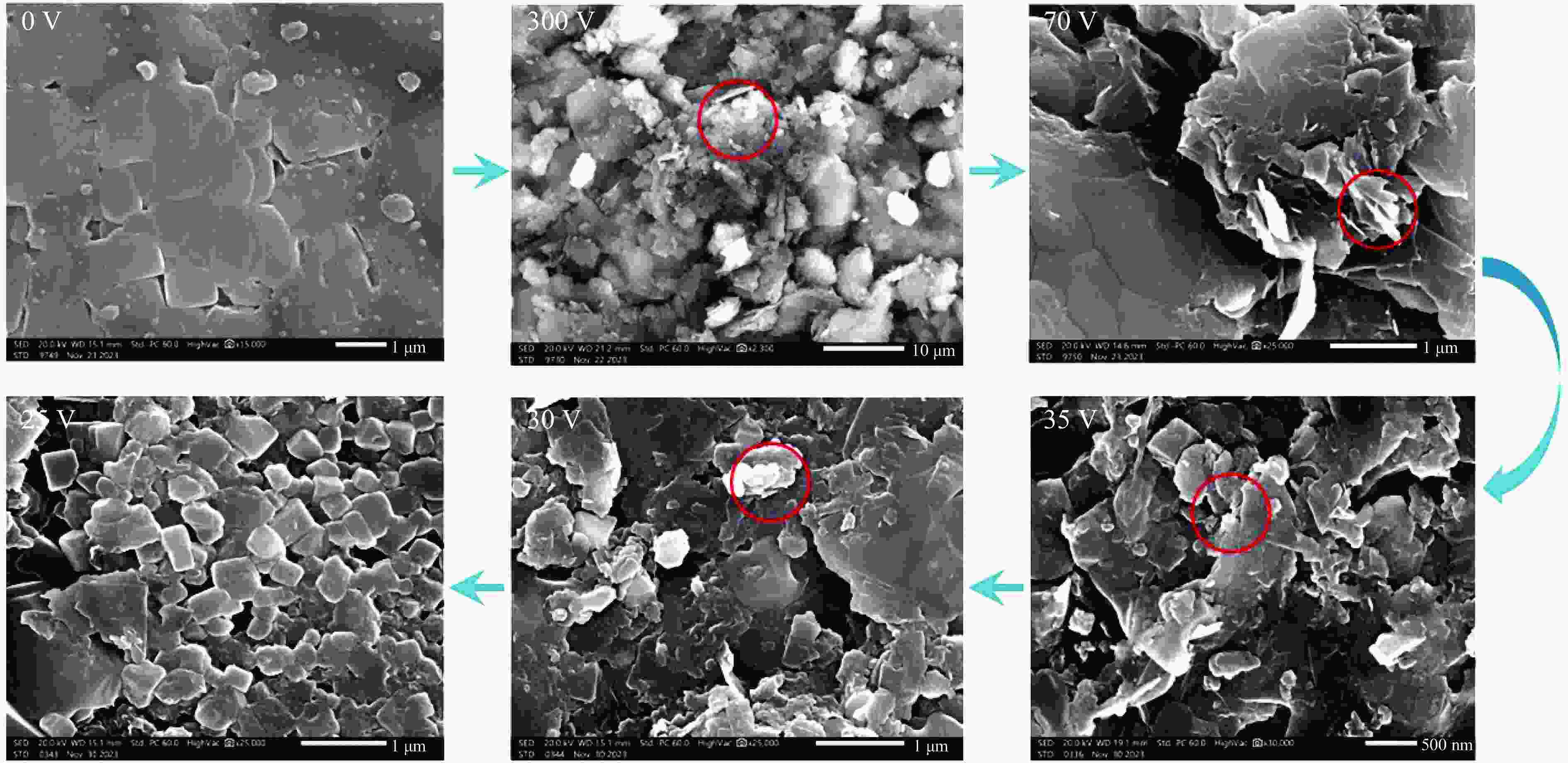
图 2 在(3.4±0.2) GPa压力下NaCl经过不同电压瞬间放电后样品的SEM图像(红圈部分为出现细晶的位置, 300 V时有非常明显的细晶现象。70、35、30 V时均出现细晶现象,说明在此电压下温度达到了NaCl的熔点。当电压降至25 V时,在SEM图像中未发现晶粒细化现象,只观察到晶粒因挤压作用而破碎,说明NaCl在3.4 GPa下的熔化电压在25~30 V之间,约为(27.5±2.5) V,此压力下NaCl的熔点为
1582 K,即 27.5 V的电压使样品腔的瞬间温度达到约1582 K。)Figure 2. SEM images of NaCl samples after flash-heating with different voltages under (3.4±0.2) GPa (The red circled areas indicate the locations where fine grains are observed, with a distinct grain refining at 300 V. Multiple experiments are conducted, sequentially reducing the voltage to 70, 35, and 30 V, all of which resulted in the appearance of fine grains, demonstrating that at such voltages, the temperature is above the melting point of NaCl. When the voltage reduced to 25 V, no fine-grained areas can be identified in the SEM image; instead, only fragmented grains due to pressure are observed. This suggests that the melting voltage of NaCl under 3.4 GPa is between 25 and 30 V, approximately (27.5±2.5) V. At this pressure, the melting point of NaCl is
1582 K, suggesting that a voltage of 27.5 V induces an instantaneous temperature of approximately1582 K in the sample chamber.)图 3 3.4 GPa下KCl瞬间放电后的SEM图像(21 V时未发现晶粒细化现象,而在25 V时发现红圈处的晶粒细化现象,说明KCl在3.4 GPa压力下的熔化电压在21~25 V之间,约为(23±2) V,此压力下KCl的熔点为
1416 K,即 23 V的电压使样品腔的瞬间温度达到约1416 K。)Figure 3. SEM images of KCl samples after flash-heating under 3.4 GPa (No grain refinement was observed at 21 V, but appeared at 25 V within the red-circled areas. It indicates that the melting voltage of KCl under 3.4 GPa is between 21 and 25 V, approximately (23±2) V. At this pressure, the melting point of KCl is
1416 K, suggesting that a voltage of 23 V induces an instantaneous temperature of approximately1416 K in the sample chamber.)图 4 3.4 GPa下Al2O3瞬间放电后的SEM图像(46 V时未发现晶粒细化现象,而在51 V时发现红圈处的晶粒细化现象,说明Al2O3在3.4 GPa下的熔化电压在46~51 V之间,约为(48.5±2.5) V,此压力下Al2O3的熔点为
2701 K,即 48.5 V的电压使样品腔的瞬间温度达到约2701 K。)Figure 4. SEM images of Al2O3 samples after flash-heating under 3.4 GPa (No grain refinement was observed at 46 V, but appeared at 51 V within the red-circled areas. It indicates that the melting voltage of Al2O3 under 3.4 GPa is between 46 and 51 V, approximately (48.5±2.5) V. At this pressure, the melting point of Al2O3 is
2701 K, suggesting that a voltage of 48.5 V induces an instantaneous temperature of approximately2701 K in the sample chamber.)图 5 3.4 GPa下MgO瞬间放电后的SEM图像(65 V时未发现晶粒细化现象,而70 V时发现红圈处的晶粒细化现象,说明MgO在3.4 GPa下的熔化电压在65~70 V之间,约为(67.5±2.5) V,此压力下MgO的熔点为
3419 K,即 67.5 V的电压使样品腔的瞬间温度达到约3419 K。)Figure 5. SEM images of MgO samples after flash-heating under 3.4 GPa (No grain refinement was observed at 65 V, but appeared at 70 V within the red-circled areas. It indicates that the melting voltage of MgO under 3.4 GPa is between 65 and 70 V, approximately (67.5±2.5) V. At this pressure, the melting point of MgO is
3419 K, suggesting that a voltage of 67.5 V induces an instantaneous temperature of approximately3419 K in the sample chamber.)图 7 3.4 GPa下h-BN经过不同电压瞬间放电后样品的SEM图像(红圈部分为细晶出现的位置。300 V时,有非常明显的晶粒细化现象;96 V时,仍能观察到晶粒细化现象;而90 V时,未见晶粒细化区域,说明在该压力下h-BN熔化,对应的电压约为(93±3) V,对应的熔化温度为(
4251 ±150) K。)Figure 7. SEM images of h-BN samples after flash-heating at different voltages under 3.4 GPa (The red circled areas indicate the locations where fine grains are observed, with a distinct grain refining at 300 V. Grain refinement is still observable at 96 V, but cannot be observed at 90 V. It indicates that the melting voltage of h-BN under this pressure is approximately (93±3) V. The corresponding melting temperature is approximately (
4251 ±150) K.)图 8 4.3 GPa下h-BN经瞬间放电后样品的SEM图像(97 V时,未发现晶粒细化现象,而105 V时,红圈处出现晶粒细化现象,说明在该压力下,h-BN的熔化电压约为(101±4) V,对应的熔化温度为(
4531 ±200) K。)Figure 8. SEM images of h-BN samples after flash-heating at 4.3 GPa (No grain refinement is observed at 97 V, but appeared at 105 V within the red-circled areas. It suggests that the melting voltage of h-BN under this pressure is approximately (101±4) V. The corresponding melting temperature is approximately (
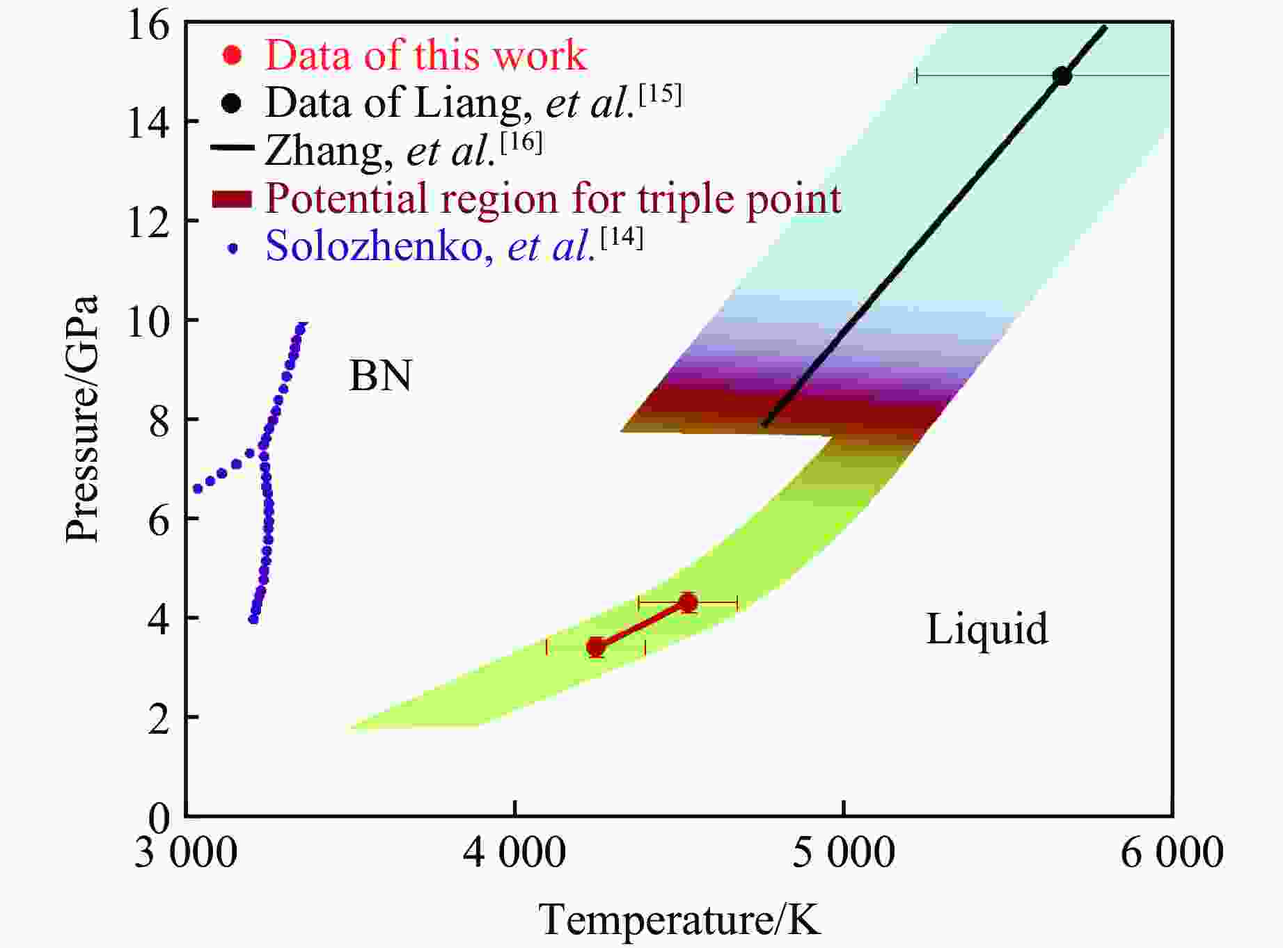
4531 ±200) K.)图 9 实验得到的c-BN的熔化数据与Zhang等[16]得到的数据的延伸和比较(蓝色区域为c-BN熔化曲线可能存在的区间,绿色区域为本实验得出的h-BN熔化曲线可能存在的区间,中间红色区域为三相点可能存在的范围。h-BN的熔化温度随压力的升高而升高,且斜率逐渐增大,但不为负值,与Solozhenko 等[14] 预测的结果不同。)
Figure 9. Extension and comparison of the results obtained in this study with data of Zhang et al.[16] on the melting curve of c-BN (The blue region indicates the possible range of the c-BN melting curve, the green region represents the possible range of the h-BN melting curve obtained from this study, and the middle red region indicates the possible range of the triple point. The melting point of h-BN is expected to increase with pressure, with the slope gradually steeper but not negative. This differs from the predictions made by Solozhenko et al.[14].)
-
[1] SONG Z Y, WANG W, CAI G X, et al. Investigation of optical spectrum properties of hexagonal boron nitride from metal to dielectric transition [J]. Plasmonics, 2018, 13(2): 563–566. doi: 10.1007/s11468-017-0544-y [2] ZHOU W Y, ZUO J, ZHANG X Q, et al. Thermal, electrical, and mechanical properties of hexagonal boron nitride: reinforced epoxy composites [J]. Journal of Composite Materials, 2014, 48(20): 2517–2526. doi: 10.1177/0021998313499953 [3] PEREVISLOV S N. Structure, properties, and applications of graphite-like hexagonal boron nitride [J]. Refractories and Industrial Ceramics, 2019, 60(3): 291–295. doi: 10.1007/s11148-019-00355-5 [4] KIM T Y, SONG E H, KANG B H, et al. Hydrolyzed hexagonal boron nitride/polymer nanocomposites for transparent gas barrier film [J]. Nanotechnology, 2017, 28(12): 12LT01. doi: 10.1088/1361-6528/aa5f2e [5] TURKOGLU M, SAHIN I, SAN T. Evaluation of hexagonal boron nitride as a new tablet lubricant [J]. Pharmaceutical Development and Technology, 2005, 10(3): 381–388. doi: 10.1081/PDT-65684 [6] DECKER R, WANG Y, BRAR V W, et al. Local electronic properties of graphene on a BN substrate via scanning tunneling microscopy [J]. Nano Letters, 2011, 11(6): 2291–2295. doi: 10.1021/nl2005115 [7] REVABHAI P M, SINGHAL R K, BASU H, et al. Progress on boron nitride nanostructure materials: properties, synthesis and applications in hydrogen storage and analytical chemistry [J]. Journal of Nanostructure in Chemistry, 2023, 13(1): 1–41. doi: 10.1007/s40097-022-00490-5 [8] SHTANSKY D V, FIRESTEIN K L, GOLBERG D V. Fabrication and application of BN nanoparticles, nanosheets and their nanohybrids [J]. Nanoscale, 2018, 10(37): 17477–17493. doi: 10.1039/C8NR05027A [9] 王艳芝, 张旺玺, 孙长红, 等. 氮化硼系列材料的合成制备及应用研究进展 [J]. 陶瓷学报, 2018, 39(6): 661–671. doi: 10.13957/j.cnki.tcxb.2018.06.002WANG Y Z, ZHANG W X, SUN C H, et al. The development of the applications and synthesis of boron nitride materials [J]. Journal of Ceramics, 2018, 39(6): 661–671. doi: 10.13957/j.cnki.tcxb.2018.06.002 [10] WANG P, HE D W, WANG L P, et al. Diamond-cBN alloy: a universal cutting material [J]. Applied Physics Letters, 2015, 107(10): 101901. doi: 10.1063/1.4929728 [11] WATANABE T, SATAKA R, YAMAMOTO K. Effect of bias application on c-BN synthesis by induction thermal plasmas under atmospheric pressure [J]. Thin Solid Films, 2008, 516(13): 4462–4467. doi: 10.1016/j.tsf.2007.10.018 [12] WENTORF JR R H. Cubic form of boron nitride [J]. The Journal of Chemical Physics, 1957, 26(4): 956. doi: 10.1063/1.1745964 [13] BUNDY F P, WENTORF JR R H. Direct transformation of hexagonal boron nitride to denser forms [J]. The Journal of Chemical Physics, 1963, 38(5): 1144–1149. doi: 10.1063/1.1733815 [14] SOLOZHENKO V L, TURKEVICH V Z, HOLZAPFEL W B. Refined phase diagram of boron nitride [J]. The Journal of Physical Chemistry B, 1999, 103(15): 2903–2905. doi: 10.1021/jp984682c [15] LIANG A K, LIU Y J, SHI L T, et al. Melting temperature of diamond and cubic boron nitride at 15 gigapascals [J]. Physical Review Research, 2019, 1(3): 033090. doi: 10.1103/PhysRevResearch.1.033090 [16] ZHANG J W, LIU F M, LI S Q, et al. Recrystallization behaviour of cubic boron nitride under high pressure [J]. Journal of the European Ceramic Society, 2021, 41(16): 132–138. doi: 10.1016/j.jeurceramsoc.2021.09.036 [17] HRUBIAK R, MENG Y, SHEN G Y. Microstructures define melting of molybdenum at high pressures [J]. Nature Communications, 2017, 8(1): 14562. doi: 10.1038/ncomms14562 [18] WU H Y, ZHUANG X L, NIE Y, et al. Effect of heat treatment on mechanical property and microstructure of a powder metallurgy nickel-based superalloy [J]. Materials Science and Engineering: A, 2019, 754: 29–37. doi: 10.1016/j.msea.2019.03.064 [19] IKESUE A, AUNG Y L, YODA T, et al. Fabrication and laser performance of polycrystal and single crystal Nd: YAG by advanced ceramic processing [J]. Optical Materials, 2007, 29(10): 1289–1294. doi: 10.1016/j.optmat.2005.12.013 [20] ZHOU X F, MA D J, WANG L F, et al. Large-volume cubic press produces high temperatures above 4 000 Kelvin for study of the refractory materials at pressures [J]. Review of Scientific Instruments, 2020, 91(1): 015118. doi: 10.1063/1.5128190 [21] BOEHLER R, ROSS M, BOERCKER D B. High-pressure melting curves of alkali halides [J]. Physical Review B, 1996, 53(2): 556–563. doi: 10.1103/PhysRevB.53.556 [22] SHEN G Y, LAZOR P. Measurement of melting temperatures of some minerals under lower mantle pressures [J]. Journal of Geophysical Research: Solid Earth, 1995, 100(B9): 17699–17713. doi: 10.1029/95JB01864 [23] BOEHLER R, ROSS M, BOERCKER D B. Melting of LiF and NaCl to 1 Mbar: systematics of ionic solids at extreme conditions [J]. Physical Review Letters, 1997, 78(24): 4589–4592. doi: 10.1103/PhysRevLett.78.4589 [24] KIMURA T, OHFUJI H, NISHI M, et al. Melting temperatures of MgO under high pressure by micro-texture analysis [J]. Nature Communications, 2017, 8(1): 15735. doi: 10.1038/ncomms15735 -


 下载:
下载:


