First Principles Study on the Electronic Structure and Optical Properties of Graphene/MoS2 Heterojunctions with Different Rotation Angles
-
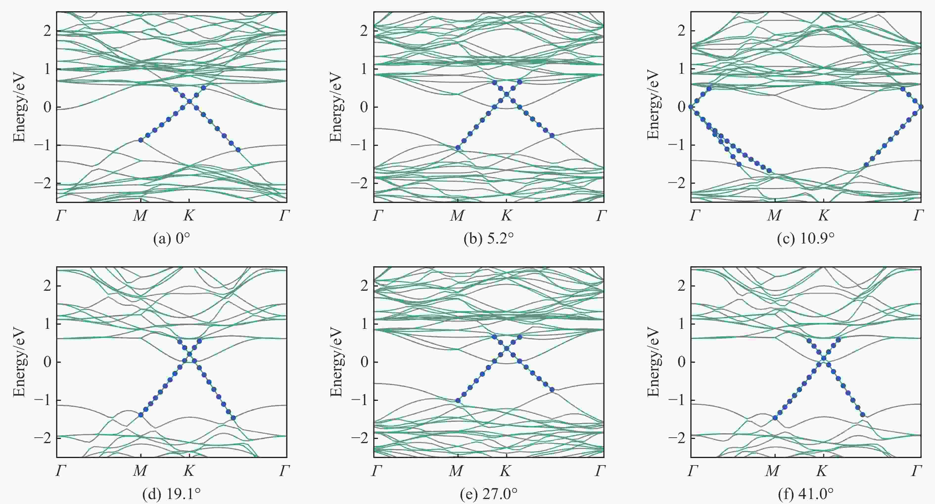
摘要: 基于密度泛函理论的第一性原理计算方法,研究了不同扭转角下石墨烯/MoS2异质结构的电子结构和光学特性。结果表明,转角后的石墨烯/MoS2异质结构仍具备作为单层材料时的部分特征。在费米能级附近,石墨烯层保持了其特殊的线性色散能带结构,狄拉克锥上的直接带隙Eg受到层间旋转调制的影响。异质结构中的MoS2层对层厚具有高度的敏感性,随着厚度的增加,其间接带隙持续增大。当转角为10.9°时, Eg的最大值为11.67 meV。差分电荷密度计算结果表明,随着旋转角度的改变,MoS2层中Mo-S间的电子转移引起了Mo―S键长的变化,从而增大了S-S层间距。同时,通过与MoS2结合形成异质结构,石墨烯获得了较高的载流子浓度,异质结界面间旋转使空穴掺杂载流子浓度提高至9.2×1012 cm−2,比未转角时提高约6倍。异质结构的光学性质计算结果表明:当转角为27.0°时,其吸收边发生红移,并向低能区移动了0.233 eV;当转角为10.9°时,其吸收边发生蓝移,并向高能区移动0.116 eV,同时,在可见光范围内,异质结构损失函数下降了0.007。研究结果可为设计新型具有转角特征石墨烯异质结构的光学纳米器件提供理论参考。
-
关键词:
- 石墨烯/MoS2异质结 /
- 光学性质 /
- 电子结构 /
- 扭转角 /
- 载流子浓度
Abstract: Based on the density functional theory (DFT), first-principles calculations were performed to investigate the electronic structures and optical properties of graphene/MoS2 heterostructures at several different twist angles. The results indicate that the twisted graphene/MoS2 heterostructures still preserve some characteristics inherent in monolayer structure. Near the Fermi level, the characteristic linear dispersion band structure of graphene layer is retained, and the direct bandgap (Eg) at the Dirac cone is influenced by interlayer rotation modulation. The bandgap of MoS2 layer exhibits a high sensitivity to layer thickness that the indirect bandgap continuously increases with the increase thickness. At a twist angle of 10.9°, the maximum value of Eg reaches 11.67 meV. The calculated differential charge density result indicates that with the interlayer rotations the Mo―S bond length is changed by the electron transfer between Mo and S atoms, resulting in a increasing of S-S interlayer distance. Simultaneously, the carrier concentration of graphene is increased when it forms a heterostructure with MoS2. The rotation at the heterojunction interface increases the hole-doped carrier concentration to 9.2×1012 cm−2, approximately six times higher than that without twist angle. The results of the optical property calculations for the heterostructures indicate that at a twist angle of 27.0°, its absorption edge undergoes a redshift to the lower energy by 0.233 eV. At a twist angle of 10.9°, the absorption edge undergoes a blue shift, moving towards the higher energy by 0.116 eV. Within the visible light range, the loss function of graphene/MoS2 heterostructure decreases by 0.007. This study can provide a theoretical basis for the design of new rotation graphene heterostructures optical nanodevices. -
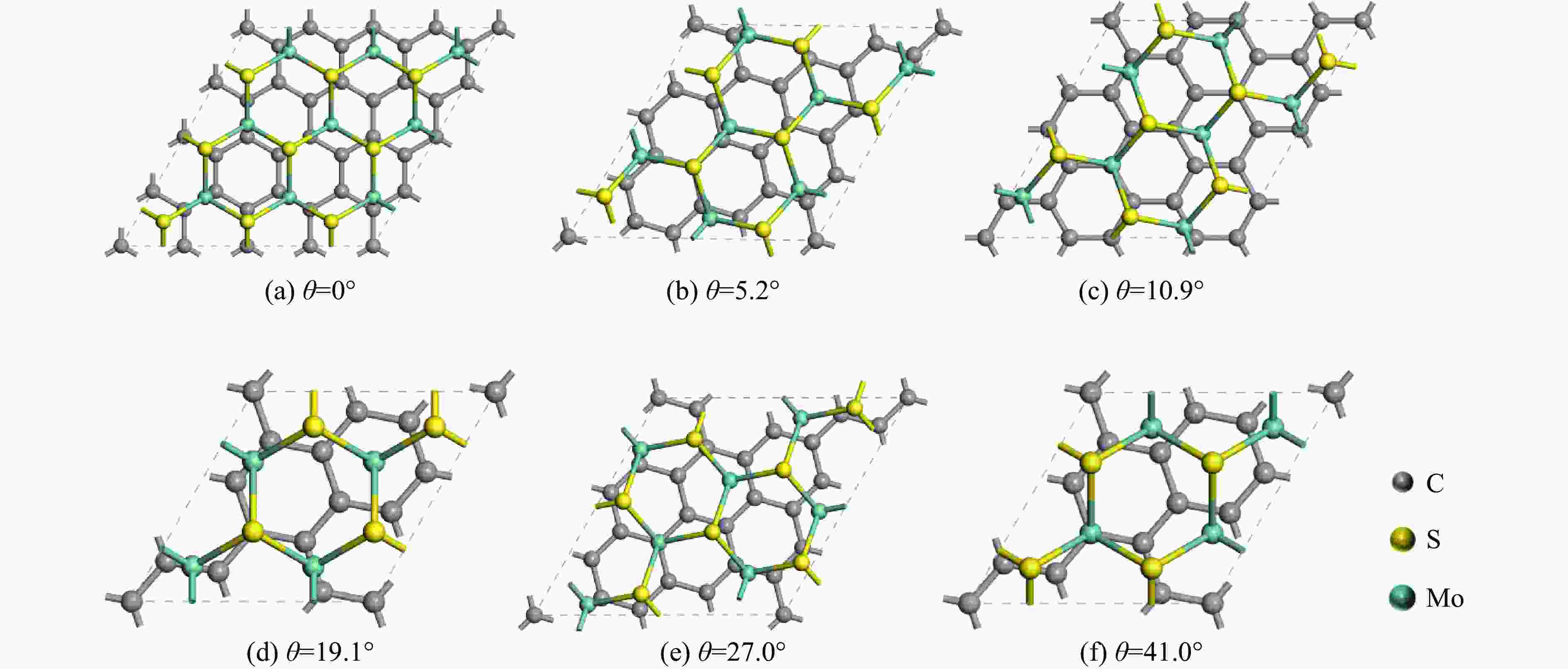
图 1 不同转角石墨烯/MoS2异质结结构示意图:(a) 石墨烯/MoS2转角结构示意图,(b) 转角石墨烯/MoS2异质结及原胞布里渊区示意图(紫色代表石墨烯,红色代表MoS2)
Figure 1. Schematic diagrams of graphene/MoS2 heterojunction structures with different twist angles: (a) graphene/MoS2 twisted structure; (b) twisted graphene/MoS2 heterojunction and Brillouin zone of its primitive cell(where purple represents graphene and red represents MoS2)
表 1 6种转角石墨烯/MoS2异质结的结构参数
Table 1. Structural parameters of six graphene/MoS2 heterojunctions
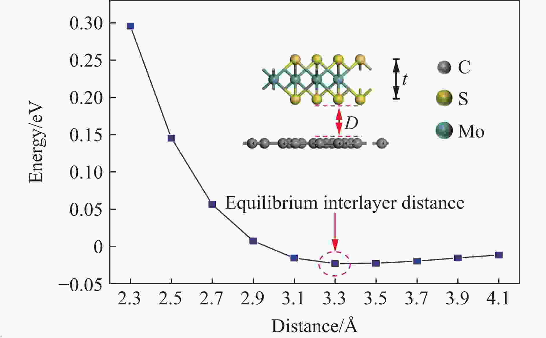
θ/(°) Eb/meV D/Å $\sigma$/% θ/(°) Eb/meV D/Å $\sigma$/% 0 –37.2 3.173 2.90 19.1 –38.6 3.482 2.14 5.2 –36.6 3.224 4.98 27.0 –36.1 3.218 4.98 10.9 –38.8 3.468 1.13 41.0 –36.8 3.250 2.14 -
[1] NOVOSELOV K S, GEIM A K, MOROZOV S V, et al. Electric field effect in atomically thin carbon films [J]. Science, 2004, 306(5696): 666–669. doi: 10.1126/science.1102896 [2] NETO A H C, GUINEA F, PERES N M R, et al. The electronic properties of graphene [J]. Reviews of Modern Physics, 2009, 81(1): 109–162. doi: 10.1103/RevModPhys.81.109 [3] 高琦璇, 钟浩源, 周树云. 二维材料的新奇物理及异质结的能带调控 [J]. 物理, 2022, 51(5): 310–318.GAO Q X, ZHONG H Y, ZHOU S Y. Novel physics of two-dimensional materials and band structure engineering in van der Waals heterostructures [J]. Physics, 2022, 51(5): 310–318. [4] WANG E Y, LU X B, DING S J, et al. Gaps induced by inversion symmetry breaking and second-generation Dirac cones in graphene/hexagonal boron nitride [J]. Nature Physics, 2016, 12(12): 1111–1115. doi: 10.1038/nphys3856 [5] ZHOU S Y, GWEON G H, FEDOROV A V, et al. Substrate-induced bandgap opening in epitaxial graphene [J]. Nature Materials, 2007, 6(10): 770–775. doi: 10.1038/nmat2003 [6] KIM S, IHM J, CHOI H J, et al. Origin of anomalous electronic structures of epitaxial graphene on silicon carbide [J]. Physical Review Letters, 2008, 100(17): 176802. doi: 10.1103/PhysRevLett.100.176802 [7] DENG S, LI L J, REES P. Graphene/MoXY heterostructures adjusted by interlayer distance, external electric field, and strain for tunable devices [J]. ACS Applied Nano Materials, 2019, 2(6): 3977–3988. doi: 10.1021/acsanm.9b00871 [8] CHEN H, ZHAO J F, HUANG J D, et al. Computational understanding of the structural and electronic properties of the GeS-graphene contact [J]. Physical Chemistry Chemical Physics, 2019, 21(14): 7447–7453. doi: 10.1039/C9CP00374F [9] PHUC H V, HIEU N N, HOI B D, et al. Interlayer coupling and electric field tunable electronic properties and Schottky barrier in a graphene/bilayer-GaSe van der Waals heterostructure [J]. Physical Chemistry Chemical Physics, 2018, 20(26): 17899–17908. doi: 10.1039/C8CP02190B [10] LI L, ZHANG L T, LAN Y, et al. Cooperative effect of strain and electric field on Schottky barriers in van der Waals heterostructure of graphene and hydrogenated phosphorus carbide [J]. Physica E: Low-dimensional Systems and Nanostructures, 2023, 148(19): 115665. [11] SINGH S, ESPEJO C, ROMERO A H. Structural, electronic, vibrational, and elastic properties of graphene/MoS2 bilayer heterostructures [J]. Physical Review B, 2018, 98(15): 155309. doi: 10.1103/PhysRevB.98.155309 [12] DENG S, ZHANG Y, LI L J. Study on electronic and optical properties of the twisted and strained MoS2/PtS2 heterogeneous interface [J]. Applied Surface Science, 2019, 476: 308–316. doi: 10.1016/j.apsusc.2019.01.097 [13] QIU B, ZHAO X W, HU G C, et al. Optical properties of graphene/MoS2 heterostructure: first principles calculations [J]. Nanomaterials, 2018, 8(11): 962–971. doi: 10.3390/nano8110962 [14] SEGALL M D, LINDAN P J D, PROBERT M J, et al. First-principles simulation: ideas, illustrations and the CASTEP code [J]. Journal of Physics: Condensed Matter, 2002, 14(11): 2717–2744. doi: 10.1088/0953-8984/14/11/301 [15] PERDEW J P, CHEVARY J A, VOSKO S H, et al. Atoms, molecules, solids, and surfaces: applications of the generalized gradient approximation for exchange and correlation [J]. Physical Review B, 1992, 46(11): 6671–6687. doi: 10.1103/PhysRevB.46.6671 [16] PERDEW J P, BURKE K, ERNZERHOF M. Generalized gradient approximation made simple [J]. Physical Review Letters, 1996, 77(18): 3865–3868. doi: 10.1103/PhysRevLett.77.3865 [17] NAIMER T, ZOLLNER K, GMITRA M, et al. Twist-angle dependent proximity induced spin-orbit coupling in graphene/transition metal dichalcogenide heterostructures [J]. Physical Review B, 2021, 104(19): 195156. doi: 10.1103/PhysRevB.104.195156 [18] GRIMME S. Semiempirical GGA-type density functional constructed with a long-range dispersion correction [J]. Journal of Computational Chemistry, 2006, 27(15): 1787–1799. doi: 10.1002/jcc.20495 [19] LI L Y, ZHAO M W. Structures, energetics, and electronic properties of multifarious stacking patterns for high-buckled and low-buckled silicene on the MoS2 substrate [J]. The Journal of Physical Chemistry C, 2014, 118(33): 19129–19138. doi: 10.1021/jp5043359 [20] PIERUCCI D, HENCK H, AVILA J, et al. Band alignment and minigaps in monolayer MoS2-graphene van der Waals heterostructures [J]. Nano Letters, 2016, 16(7): 4054–4061. doi: 10.1021/acs.nanolett.6b00609 [21] LI Y T, XIAO H P, ZHOU P, et al. Electronic structures of twist-stacked 1T-TaS2 bilayers [J]. Physics Letters A, 2019, 383(19): 2302–2308. doi: 10.1016/j.physleta.2019.04.043 [22] EBNONNASIR A, NARAYANAN B, KODAMBAKA S, et al. Tunable MoS2 bandgap in MoS2-graphene heterostructures [J]. Applied Physics Letters, 2014, 105(3): 031603. doi: 10.1063/1.4891430 [23] RISTEIN J, MAMMADOV S, SEYLLER T. Origin of doping in quasi-free-standing graphene on silicon carbide [J]. Physical Review Letters, 2012, 108(24): 246104. doi: 10.1103/PhysRevLett.108.246104 [24] SAHA S, SINHA T P, MOOKERJEE A. Electronic structure, chemical bonding, and optical properties of paraelectric BaTiO3 [J]. Physical Review B, 2000, 62(13): 8828–8834. doi: 10.1103/PhysRevB.62.8828 [25] YANG G, GAO S P. A method to restore the intrinsic dielectric functions of 2D materials in periodic calculations [J]. Nanoscale, 2021, 13(40): 17057–17067. doi: 10.1039/D1NR04896A [26] YANG G, FAN J C, GAO S P. Momentum and thickness dependent excitonic and plasmonic properties of 2D h-BN and MoS2 restored from supercell calculations [J]. Nanoscale Advances, 2023, 5(24): 6990–6998. doi: 10.1039/D3NA00670K -


 下载:
下载:


